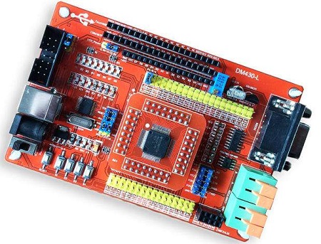
The MSP430 microcontroller is a mixed-signal processor. It provides a single-chip solution by integrating several different functional analog circuits, digital circuit modules, and microprocessors on a single chip for practical application requirements. This series of microcontrollers are mostly used in portable instrumentation that requires battery power.

MSP430 Microcontroller
Ⅰ MSP430 microcontroller features
The rapid development of the MSP430 series of microcontrollers and the expanding range of applications mainly depends on the following characteristics.
a. Powerful processing capability
MSP430 series microcontroller is a 16-bit microcontroller, using a compact instruction set (RISC) structure, with a rich addressing mode (7 source operand addressing, 4 destination operand addressing), concise 27 kernel instructions, and a large number of analog instructions; a large number of registers and on-chip data memory can participate in a variety of operations; there is also a highly efficient look-up table processing instructions. These features ensure that highly efficient source programs can be produced.
b. Fast computing speed
In terms of computing speed, the MSP430 series microcontroller can achieve 125ns instruction cycle driven by 8MHz crystal. 16-bit data width, 125ns instruction cycle and multi-function hardware multiplier (multiply and add) together, can achieve some algorithms of digital signal processing (such as FFT, etc.).
c. More interrupt sources
MSP430 series microcontroller has more interrupt sources and can be arbitrarily nested, flexible and convenient to use. When the system is in a power-saving standby state, it only takes 6us to wake it up with an interrupt request.

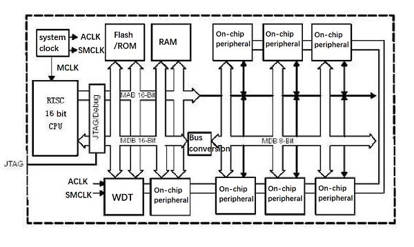
MSP430 Microcontroller structure
d. Ultra-low power consumption
MSP430 microcontroller has ultra-low power consumption because of its unique features in reducing the chip's supply voltage and flexible and controllable operating clock.
First, the MSP430 series microcontroller power supply voltage is 1.8 ~ 3.6V voltage. Therefore, it can run at lMHz clock conditions. The chip current will be about 200 ~ 400uA, the clock off mode of the lowest power consumption of 0.1uA.
Second, the unique clock system design. In the MSP430 family, there are two different system clock systems: the basic clock system and frequency-locked loop (FLL and FLL+) clock system or DCO digital oscillator clock system. Some use one crystal oscillator (32768Hz) and some use two crystal oscillators). The clocks required for each function are generated by the system clock system. And these clocks can be turned on and off under the control of instructions, thus enabling control of the overall power consumption.
The power consumption of the chip has a significant difference due to the different functional modules that are turned on when the system is running, i.e., different operating modes are used. There is one active mode (AM) and five low-power modes (LPMO~LPM4) in the system. In the wait mode, the power consumption is 0.7uA, and in the power saving mode, it can be as low as 0.1uA.
e. Stable system operation
After power-on reset, the CPU is first started by DCOCLK to ensure that the program starts to execute from the correct position and that the crystal oscillator has enough starting and stabilization time. Then the software can set the control bits of the appropriate registers to determine the final system clock frequency. If the crystal oscillator fails when used as the CPU clock MCLK, the DCO will automatically start to ensure the system works properly; if the program runs away, the watchdog can be used to reset it.
f. Rich on-chip peripheral modules
Members of the MSP430 series microcontroller are integrated with rich on-chip peripherals. They are watchdog (WDT), analog comparator A, timer A (TimerA), timer B (TimerB), serial ports 0, 1 (USART0, 1), hardware multiplier, LCD driver, l 0-bit/l 2-bit ADC, I2C, bus direct data access (DMA), port 0 (P0), ports 1 to 6 (P1 to P6), basic timer (Bas i c Timer) and some other peripheral modules in different combinations.
g. Convenient and efficient development environment
At present, the MSP430 series has three types of devices, OPT type, FLASH type, and ROM type. These devices have different development means. For OPT type and ROM type devices are developed using emulators after the successful burn-in or mask chip. FLASH type has a very convenient development and debugging environment. Because the device has an on-chip JTAG debug interface and electrically erasable FLASH memory, we use the method of developing by downloading the program to FLASH first, then controlling the operation of the program through software in the device, and reading the information in the chip by the JTAG interface for the designer to debug. This approach requires only a PC and a JTAG debugger instead of an emulator and programmer.
h. Adapt to the industrial-grade operating environment
MSP430 series devices are industrial-grade, operating environment temperature of 40 ~ +85 degrees Celsius. The products can be designed for use in industrial environments.
Ⅱ How do I learn MSP430 microcontroller?
(1) Access to information
Purchase the relevant books. On the Internet, you can find the FET use guide, MSP430 F1xx series, F4xx series instructions, and specific microcontroller chip data description, as well as the emulator FET circuit diagram, experimental board circuit diagram, knowledge of chip packaging, and a large number of practical applications, reference circuit.
(2) Purchase emulator FET and experimental board
(3) Homemade emulator FET and experimental board
(4) Obtain IAR software from the Internet
Go to TI's website to download the IAR software and install it on your computer.
(5) Debug FET and experimental board
Connect one end of the FET to the parallel port of the PC and the other end to the JTAG interface of the experimental board. After power on, check whether the FET chip, the experimental board on the microcontroller chip is hot. After the PC is working properly, run the IAR software, find a C language or assembly language examples, compile successfully, and download to the microcontroller. If you can download, it means that everything is successful.
(6) Step-by-step learning microcontroller
Learning to use a microcontroller means understanding the hardware structure of a microcontroller. Learning to set up the initialization of various functions in assembly or C, and programming to implement various functions.
Step 1: the use of digital I/O
The digital I/O function of the pins can be learned by using the button input signal and the to display the output level. After a button is pressed, a certain light-emitting diode glows, which is the function of combinational logic in a digital circuit. Although it is very simple, you can learn the general microcontroller programming ideas, for example, many registers must be set to initialize the pins in order to make the pins have digital input and output functions. Every time you use a function of the microcontroller, you have to set up the registers that control that function, which is the characteristic of microcontroller programming.
Step 2: the use of the timer
Learn to use the timer, you can use the microcontroller to implement the timing circuit. Timing circuits are powerful and have many applications in the control of industrial and household electrical equipment. Digital can implement timing circuits, and programmable logic devices (PLDs) can implement timing circuits. Programmable controllers (PLCs) can also implement timing circuits, but only microcontrollers are the easiest and least expensive to implement. The use of timers is very important, and logic plus time control is the basis for the use of microcontrollers.
Step 3: Interrupt
The microcontroller is characterized by the repeated execution of a program, and the execution of each instruction in the program requires a certain amount of execution time. If the program does not execute to a certain instruction, the action of that instruction will not happen, which will delay a lot of things that happen quickly. To make the microcontroller react to fast actions during the normal operation of the program, it is necessary to use the interrupt function of the microcontroller. This function means that the microcontroller interrupts the normally running program after a fast action occurs to process the fast occurring action. After the processing is complete, in return to execute the normal program.
Step 4: RS232 communication with PC
Microcontrollers have USART interfaces. The MSP430 series in many models have two USART interface. USART interface can not be directly connected to the PC RS232 interface, the logic level between them is different, you need to use a MAX3232 chip for level conversion.
The use of the USART interface is very important. Through the interface, it allows the exchange of information between the microcontroller and the PC. Although RS232 communication is not advanced, it is very important for the learning of the interface. For the correct use of the USART interface, you need to learn the communication protocol, the PC RS232 interface programming, and other knowledge.
Step 5: Learn A/D conversion
MAP430 microcontroller with multi-channel 12-bit A/D converter, through these A/D converters, allows the microcontroller to operate analog, display, and detect voltage, current, and other signals. Learn to pay attention to the concepts of analog ground and digital ground, reference voltage, sampling time, conversion rate, conversion error, etc.
Step 6: Learn PCI, I2C interface, and LCD interface
The use of these interfaces can make the microcontroller easier to connect to external devices and is very important in extending the functionality of the microcontroller.
Step 7: Learn the comparison, capture, and PWM functions
These functions can enable the microcontroller to control the motor, detect the speed signal, realize the motor governor, and other control up functions.
Step 8: Learn USB interface, TCP/IP interface, hardware and software design of various industrial buses
It is very important to learn the hardware and software design of USB interfaces, TCP/IP interfaces, and various industrial buses because this is the current development direction of product development.
Recommendations
-
Tel
13824346118 -
Whatsapp

 ENGLISH
 简体中文
简体中文